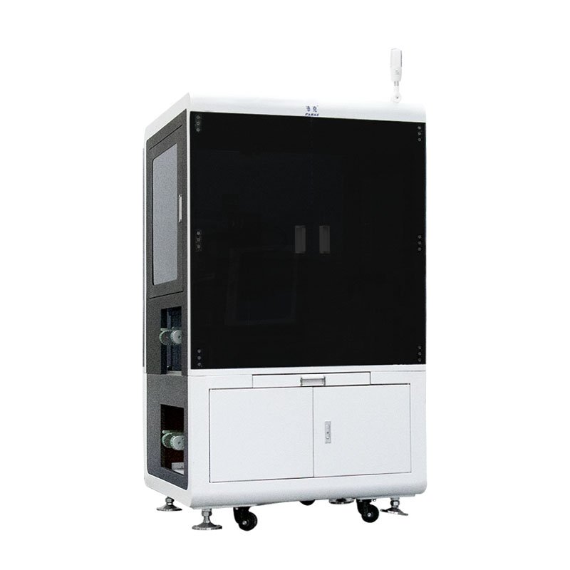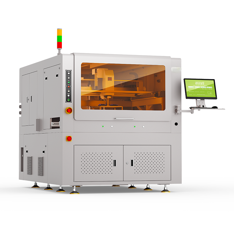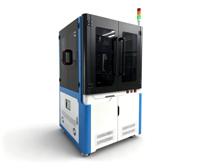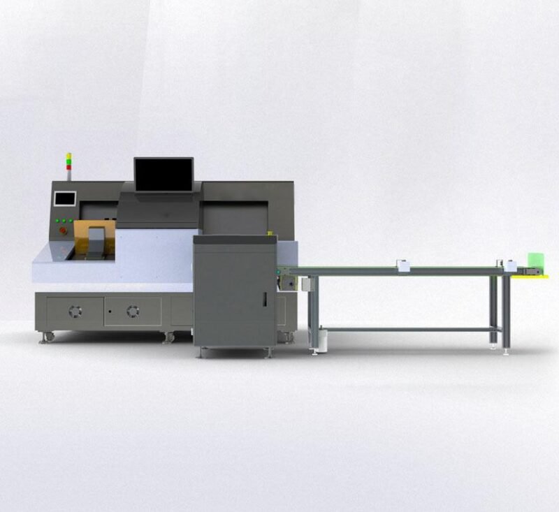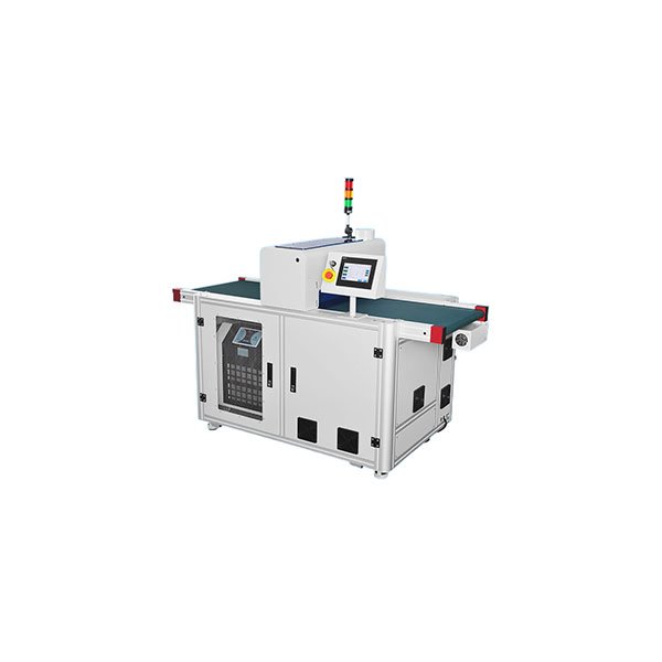
Electronic manufacturing relies on flawless surface adhesion and cleanliness for product reliability, and the Wide-Width Atmospheric Plasma Cleaner delivers this efficiently. It solves adhesion issues and contamination problems without chemicals, supporting high-volume production lines.
PCB & FPC Production: Enhancing Bonding & Reliability
Firstly, PCBs and FPCs accumulate flux residues, oxidation, and dust during fabrication, which harm soldering and bonding. The Wide-Width Atmospheric Plasma Cleaner removes these contaminants and activates surfaces, boosting copper foil surface energy significantly.
Moreover, its wide processing width (up to 800mm) matches PCB panel sizes, enabling in-line integration. This solution reduces焊接 defects from 8% to 0.5% and improves HDI board via reliability by eliminating drill smear.
Display Panel Manufacturing: Reducing Bonding Bubbles
LCD and OLED panels require perfect bonding between glass and touch modules. The Wide-Width Atmospheric Plasma Cleaner treats surfaces before lamination, minimizing bubbles caused by organic contaminants.
Additionally, it lowers the surface contact angle to below 20°, enhancing OCA optical adhesive adhesion. This solves the common issue of post-lamination bubble reoccurrence, cutting rework rates by over 60%.
Semiconductor Packaging: Boosting Bonding Strength
Secondly, semiconductor packaging (wire bonding, flip-chip) needs oxide-free, activated surfaces for strong connections. The Wide-Width Atmospheric Plasma Cleaner removes resin residues from solder bumps and cleans lead frames gently.
Furthermore, its low-temperature process (below 60°C) avoids damaging sensitive components. This solution improves flip-chip bump retention by three times and doubles mold resin adhesion strength, preventing delamination.
Battery Module Production: Ensuring Electrical Safety
EV battery BMS boards and cell tabs require clean surfaces for reliable soldering and bonding. The Wide-Width Atmospheric Plasma Cleaner removes grease and oxidation without damaging热敏 elements.
For example, it increases conductive adhesive bonding strength by 300% on polyimide substrates. This solution extends battery module lifespan and raises insulation coating salt spray resistance by three times.
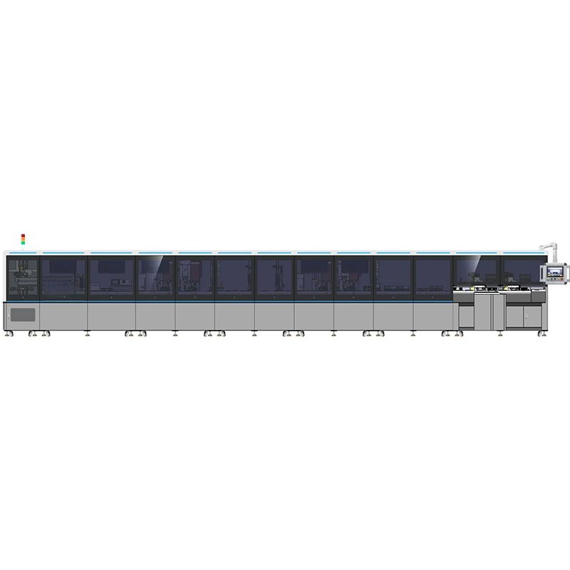
In-Line Manufacturing: Enabling Green & High-Speed Production
Finally, modern electronic factories prioritize efficiency and sustainability. The Wide-Width Atmospheric Plasma Cleaner operates at atmospheric pressure, eliminating bulky vacuum systems and cutting energy use by 40%.
Its compatibility with roll-to-roll and sheet processing (speeds up to 3m/min) supports 24/7 production. It also replaces chemical solvents, reducing annual VOCs emissions by 2.3 tons per unit, meeting RoHS standards.
Core Value: Efficiency, Quality & Sustainability in One
The Wide-Width Atmospheric Plasma Cleaner combines wide coverage, non-contact processing, and real-time monitoring. It outperforms traditional cleaning methods by balancing speed, precision, and environmental friendliness.
In electronic manufacturing, it’s not just a cleaner—it’s a solution that boosts yields, reduces costs, and enables the production of high-reliability devices from smartphones to EV components.
Jetronl Instruments Co., Ltd. has specialized in the electronic measurement field for 35 years, covering various measurement needs across the entire electronic industry chain and providing precise measurement support.