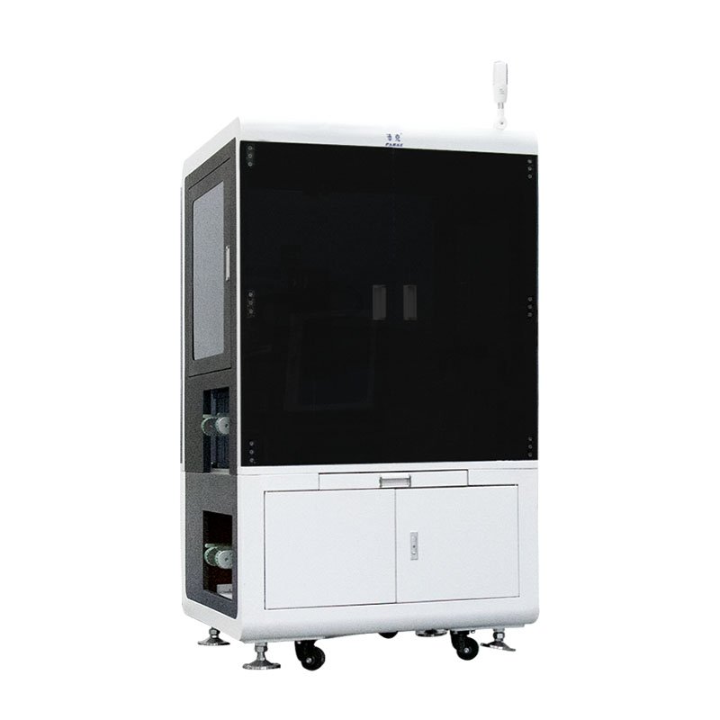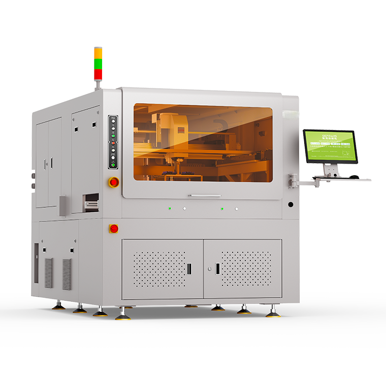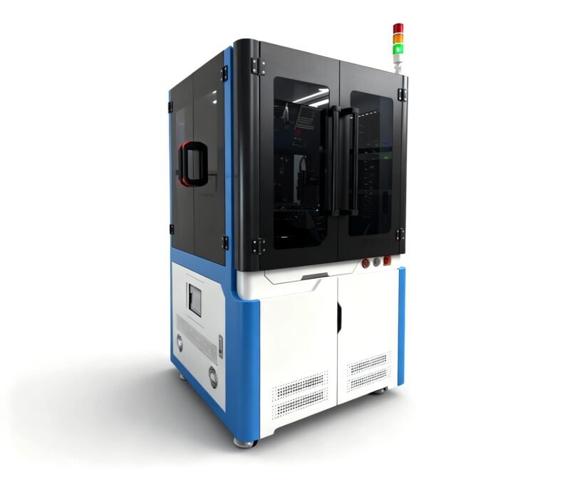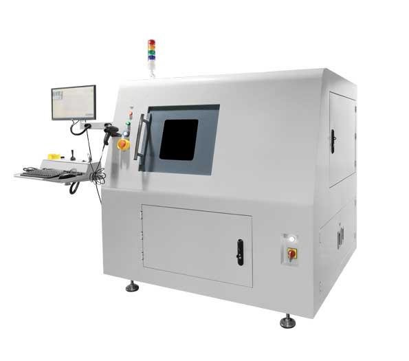
इलेक्ट्रॉनिक विनिर्माण को घनी पैकेजिंग और जटिल असेंबलियों में छिपी खामियों के साथ बढ़ती चुनौतियों का सामना करना पड़ रहा है, और यह 2.5डी एक्स-रे निरीक्षण उपकरण एक लागत प्रभावी समाधान प्रदान करता है. यह आंतरिक खामियों को उजागर करने के लिए कोणीय परिप्रेक्ष्य का उपयोग करता है जो 2डी सिस्टम में छूट जाती है, महत्वपूर्ण इलेक्ट्रॉनिक घटकों के लिए सटीकता और उत्पादन दक्षता को संतुलित करना.
श्रीमती & पीसीबी असेंबली: बीजीए को उजागर करना & छिपे हुए सोल्डर दोष
पहले तो, बीजीए, सीएसपी, और क्यूएफएन घटकों में छिपे हुए सोल्डर जोड़ होते हैं जो एओआई निरीक्षण से बचते हैं. 2.5डी एक्स-रे निरीक्षण उपकरण कोणीय छवियां उत्पन्न करने के लिए अपने एक्स-रे स्रोत को ±60° तक झुकाता है, तकिये के प्रभाव को स्पष्ट रूप से पहचानना, ठंडा सोल्डर, और इन महत्वपूर्ण कनेक्शनों में माइक्रोक्रैक.
इसके अतिरिक्त, यह ऑटोमोटिव और एयरोस्पेस पीसीबी के लिए महत्वपूर्ण सोल्डर शून्य दरों को सटीक रूप से मापता है और अत्यधिक रिक्तियों को चिह्नित करता है जो थर्मल या विद्युत विफलता का जोखिम उठाते हैं।. इस समाधान ने माइक्रोन-स्तरीय बीजीए सोल्डर पृथक्करण का पता लगाकर एक ऑटोमेकर के लिए एक प्रमुख ईसीयू संचार समस्या का समाधान किया, जो 2डी एक्स-रे से चूक गया था।, फ़ील्ड विफलताओं को काटना 70%.
सेमीकंडक्टर पैकेजिंग: आंतरिक संरचनात्मक अखंडता का सत्यापन
सेमीकंडक्टर पैकेज (जैसे वायर-बॉन्ड आईसी और फ्लिप-चिप्स) आंतरिक तारों के निरीक्षण की आवश्यकता है, मरो संलग्न, और एनकैप्सुलेशन. 2.5डी एक्स-रे निरीक्षण उपकरण वायर स्वीप की जांच के लिए एपॉक्सी केसिंग में प्रवेश करता है, स्थानान्तरित करना, और घटकों को नुकसान पहुंचाए बिना प्रदूषण.
इसके अतिरिक्त, इसकी उच्च-रिज़ॉल्यूशन इमेजिंग (4μm तक नीचे) टूटे हुए बॉन्डिंग तारों या अपर्याप्त डाई अटैच चिपकने वाले जैसे सूक्ष्म दोषों को पकड़ता है. इससे पैकेजिंग सुविधाओं को सख्त गुणवत्ता मानकों का अनुपालन करने में मदद मिलती है, अंतिम उत्पादों में प्रारंभिक चरण की घटक विफलताओं को कम करना.
उच्च घनत्व पीसीबी & एचडीआई बोर्ड परीक्षण: स्तरित जटिलता को नेविगेट करना
दूसरे, एचडीआई बोर्ड और मल्टी-लेयर पीसीबी में ओवरलैपिंग आंतरिक निशान और अंधे/दबे हुए वाया होते हैं जिनका दृश्य रूप से निरीक्षण करना असंभव है. 2.5डी एक्स-रे निरीक्षण उपकरण परतों के बीच अंतर करने के लिए मल्टी-एंगल इमेजिंग का उपयोग करता है, शॉर्ट सर्किट का पता लगाना, वाया खोलें, और इन घनी संरचनाओं में अनुचित सोल्डर भरा हुआ है.
आगे, यह एक बंद-लूप प्रणाली बनाने के लिए पीसीबी ड्रिलिंग लाइनों के साथ एकीकृत होता है, दोषों के माध्यम से आवर्ती को ठीक करने के लिए वास्तविक समय में प्रक्रियाओं को समायोजित करना. इस समाधान ने सर्वर निर्माता की पीसीबी स्क्रैप दर को कम कर दिया 22% आंतरिक परतों में छिपे ड्रिल स्मीयर और तांबे के अवशेषों की पहचान करके.
इलेक्ट्रॉनिक घटक गुणवत्ता नियंत्रण: आंतरिक खामियों की जांच
एमएलसीसी जैसे निष्क्रिय घटक, संधारित्र, और कनेक्टर्स में अक्सर आंतरिक दोष होते हैं (जैसे दरारें या विदेशी कण) जो क्षेत्र में विफलताओं का कारण बनता है. 2.5डी एक्स-रे निरीक्षण उपकरण असेंबली से पहले इन घटकों की स्क्रीनिंग करता है, संरचनात्मक कमज़ोरियों का पता लगाना जो मानक विद्युत परीक्षण में छूट जाती हैं.
उदाहरण के लिए, इसने एमएलसीसी के एक बैच को उजागर किया जिसमें खराब संचालन के कारण छिपी हुई तनाव दरारें थीं, उन्हें उपभोक्ता इलेक्ट्रॉनिक्स में उपयोग करने से रोकना और महंगी रिकॉल से बचना. सिरेमिक से लेकर प्लास्टिक तक विभिन्न सामग्रियों को संभालने की इसकी क्षमता इसे आने वाले घटकों के निरीक्षण के लिए बहुमुखी बनाती है.
उत्पादन लाइन एकीकरण: संतुलन गति & शुद्धता
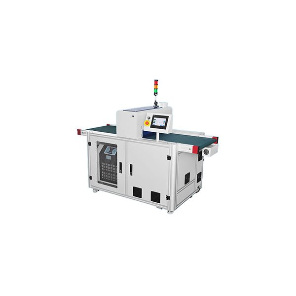
अंत में, आधुनिक इलेक्ट्रॉनिक कारखानों को ऐसे निरीक्षण उपकरणों की आवश्यकता होती है जो उच्च मात्रा में उत्पादन गति से मेल खाते हों. 2.5डी एक्स-रे निरीक्षण उपकरण सीएनसी-प्रोग्राम्ड स्वचालित बैच परीक्षण का समर्थन करता है, 400 मिमी×460 मिमी पीसीबी का निरीक्षण पूरा करना 60 0.01 मिमी माप सटीकता बनाए रखते हुए सेकंड.
इसका विकिरण उत्सर्जन कम है (<1μSv/h) कार्यस्थल सुरक्षा सुनिश्चित करता है, और एमईएस सिस्टम के साथ इसकी अनुकूलता पूर्ण दोष का पता लगाने में सक्षम बनाती है. यह समाधान धीमी गति के बीच एक मध्य मार्ग प्रदान करता है, महंगे 3डी सीटी सिस्टम और सीमित 2डी एक्स-रे, अधिकांश उच्च-मात्रा वाली उत्पादन लाइनों के लिए सही संतुलन प्रदान करना.
कोर मूल्य: आधुनिक इलेक्ट्रॉनिक्स के लिए लागत प्रभावी परिशुद्धता
2.5डी एक्स-रे निरीक्षण उपकरण कोणीय इमेजिंग क्षमता को जोड़ता है, उच्च संकल्प, और उपयोगकर्ता के अनुकूल संचालन. यह विनाशकारी परीक्षण की आवश्यकता को समाप्त करता है और ऑपरेटर अनुभव पर निर्भरता को कम करता है, सभी पारियों में लगातार दोष का पता लगाना सुनिश्चित करना.
इलेक्ट्रॉनिक विनिर्माण में, यह सिर्फ एक निरीक्षण उपकरण नहीं है - यह एक समाधान है जो उत्पाद की विश्वसनीयता की रक्षा करता है, वारंटी लागत कम कर देता है, और तेजी से लघु और जटिल इलेक्ट्रॉनिक उपकरणों के उत्पादन को सक्षम बनाता है.
जेट्रॉनल इंस्ट्रूमेंट्स कंपनी, लिमिटेड. के लिए इलेक्ट्रॉनिक माप क्षेत्र में विशेषज्ञता प्राप्त है 35 साल, संपूर्ण इलेक्ट्रॉनिक उद्योग श्रृंखला में विभिन्न माप आवश्यकताओं को कवर करना और सटीक माप समर्थन प्रदान करना.