Производство электронной и полупроводниковой промышленности полагаются на сверхточное позиционирование при микрообработке и сборке., и Рабочий стол с ЧПУ is a core component enabling this. It solves positioning inaccuracy issues, supporting the production of high-precision electronic and semiconductor products.
Semiconductor Wafer Processing: Ensuring Microfabrication Accuracy
Во-первых, semiconductor wafer etching, deposition, and dicing require nanometer-level positioning accuracy. The CNC Worktable drives wafers to precise positions, matching the processing path of laser or plasma tools.
Более того, its high repeatability (≤±1μm) ensures consistent processing across the entire wafer surface. This solution reduces wafer scrap rates by 22% and supports the production of advanced 3nm/2nm process chips.
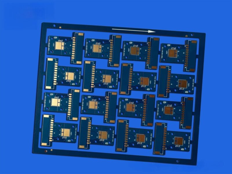
PCB Micro-Drilling & Routing: Enhancing Circuit Density
High-density PCBs (HDI boards) for smartphones and servers need tiny vias and precise routing. The CNC Worktable carries PCBs to enable micro-drilling with hole diameters as small as 0.1mm.
Кроме того, its multi-axis linkage (X/Y/Z axes) supports complex routing paths, adapting to irregular PCB layouts. This solves the problem of signal interference caused by imprecise routing, improving PCB performance.
Electronic Component Assembly: Boosting Mounting Precision
Во-вторых, miniaturized electronic components (01005 chips, micro sensors) require ultra-accurate mounting. The CNC Worktable positions circuit boards precisely during SMT assembly, matching the placement of pick-and-place machines.
Более того, its high-speed positioning (up to 500mm/s) matches the rhythm of high-volume production lines. This solution improves component mounting accuracy by 30% and reduces solder joint defects in electronic products.
Optoelectronic Component Processing: Supporting High-Precision Cutting
Optoelectronic components (светодиодные чипы, optical lenses) in electronic devices need precise cutting and polishing. The CNC Worktable fixes these fragile components, ensuring stable processing without damage.
Например, it enables laser cutting of LED chips with edge smoothness errors within 2μm. This solution enhances the light-emitting efficiency of LED components by 15% and extends their service life.
Customized Semiconductor Fixture Machining: Adapting to Diversified Needs
Окончательно, semiconductor manufacturing requires customized fixtures for different chips and wafers. The CNC Worktable processes metal or ceramic materials to produce high-precision fixtures with complex structures.
Its compatibility with multiple machining tools (milling, grinding) simplifies fixture production workflows. This solution shortens fixture development cycles by 40% and meets the diversified needs of semiconductor production.
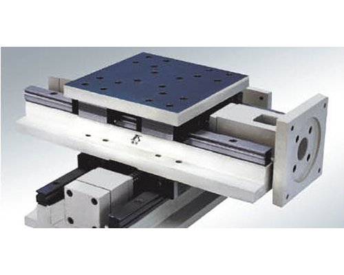
Основная ценность: Стабильность & Precision Driving Industry Advancement
The CNC Worktable combines high rigidity, ultra-precise positioning, and fast response. It adopts linear guideways and ball screws to minimize vibration during high-speed operation.
In electronic and semiconductor manufacturing, it’s not just a positioning component—it’s a solution that improves production efficiency, гарантирует качество продукции, and supports the development of high-tech electronic industries.
Компания Jetronl Instruments Co., ООО. специализируется в области электронных измерений для 35 годы, покрытие различных потребностей в измерениях во всей цепочке электронной промышленности и обеспечение точной поддержки измерений.
.jpg)