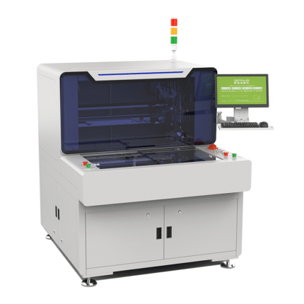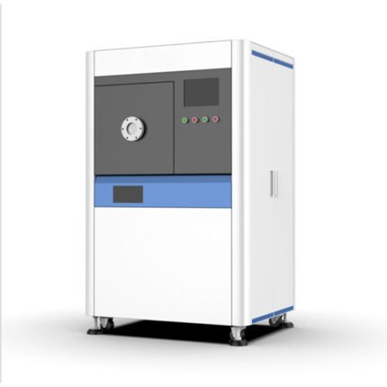
Полностью автоматическое оборудование для рентгеновского контроля
Полностью автоматическое оборудование рентгеновского контроля — это высокоточное устройство неразрушающего контроля, предназначенное для проверки внутренних структур и дефектов изделий без их повреждения.. Он использует технологию проникновения рентгеновских лучей в сочетании с автоматизированными системами для выполнения комплексных проверок таких компонентов, как электронные сборки., печатные платы, полупроводниковые корпуса, батарейки, и металлические отливки.
Основные функции
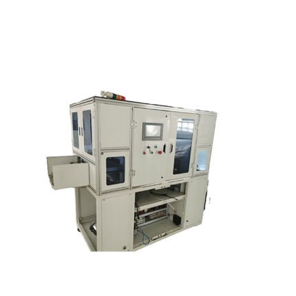
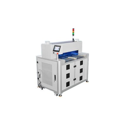
Автоматизированный процесс проверки: Интегрирует автоматическую загрузку/разгрузку., Рентгеновская визуализация, и анализ данных в единый рабочий процесс. Он может непрерывно проверять партии продукции без ручного вмешательства., значительное повышение эффективности тестирования.
Визуализация высокого разрешения: Оснащен детекторами высокого разрешения и современными источниками рентгеновского излучения., он генерирует четкие изображения внутренних структур, возможность обнаружения скрытых дефектов, таких как пустоты, трещины, расслоения, и перекосы.
Интеллектуальное распознавание дефектов: Использует алгоритмы обработки изображений на основе искусственного интеллекта для автоматического выявления и классификации дефектов., с настраиваемыми критериями для соответствия конкретным отраслевым стандартам. Он предоставляет количественные данные (например, процент недействительности, качество пайки) для объективной оценки.
Ключевые технические характеристики
Высокая точность: Достигает пространственного разрешения до нескольких микрон., обеспечение обнаружения даже микромасштабных дефектов в электронных компонентах высокой плотности.
Универсальная адаптируемость: Поддерживает различные размеры и типы продуктов, с регулируемыми рентгеновскими параметрами (Напряжение, текущий) для соответствия материалам разной толщины и плотности.
Отслеживание данных: Автоматически сохраняет изображения проверок, отчеты о дефектах, и параметры испытаний, содействие отслеживанию качества и оптимизации процессов.
Безопасность Защита: Оснащен множеством защитных блокировок., радиационная защита, и радиационный мониторинг в режиме реального времени для обеспечения безопасности оператора и соблюдения норм радиационной безопасности.
Области применения
Широко используется в производстве электроники. (проверка BGA, CSP, и паяные соединения печатных плат), полупроводниковая промышленность (проверка пластин и упаковки), производство аккумуляторов (внутренняя структура и обнаружение короткого замыкания), и производство автомобильных запчастей (проверка дефектов литья).

Полностью автоматическое оборудование для рентгеновского контроля