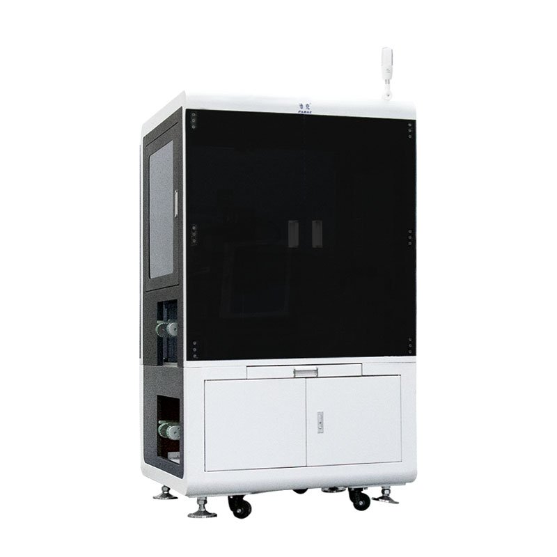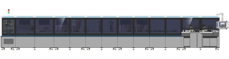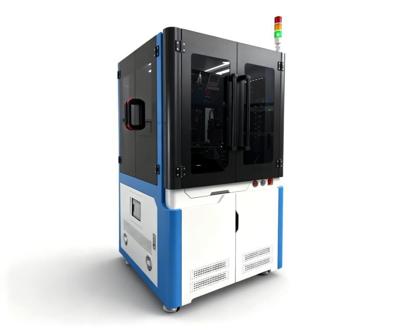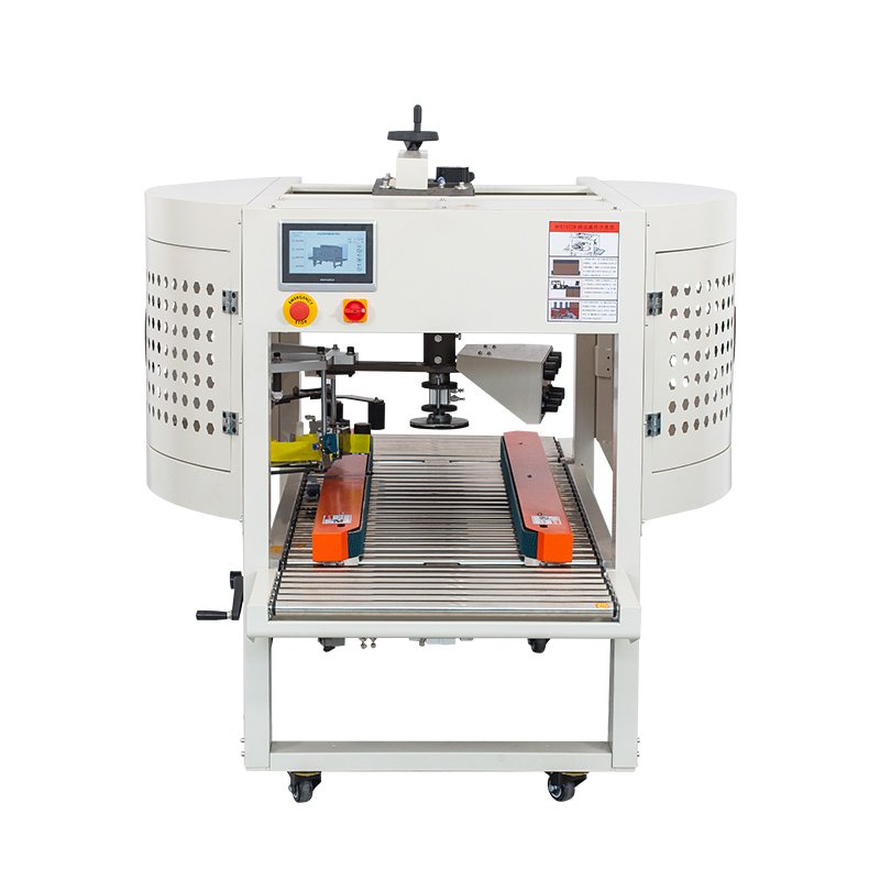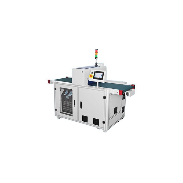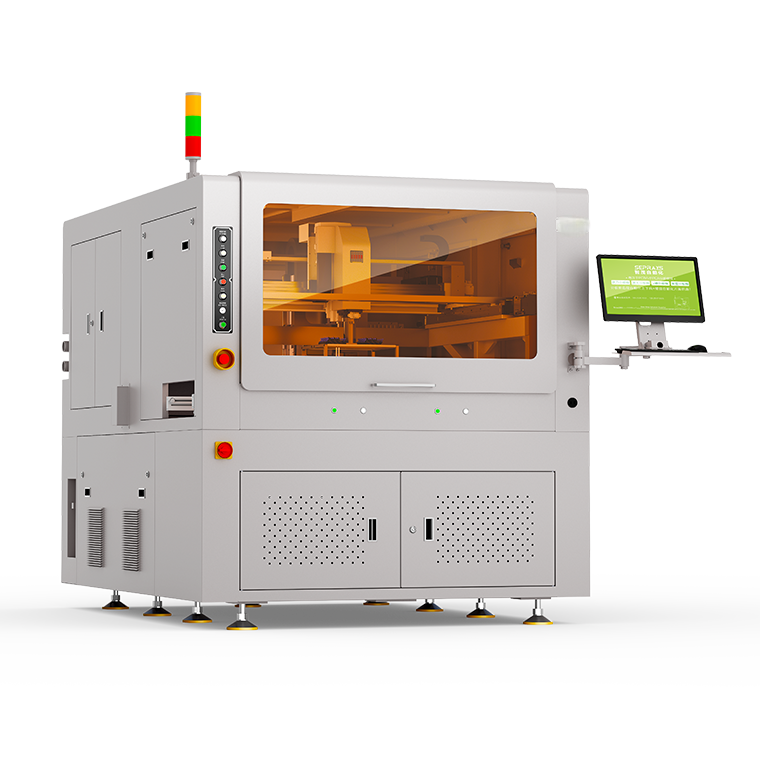
The 3C electronics industry relies on high-precision, non-damaging PCB cutting to meet miniaturization demands, and the Inline PCB Laser Depaneling Machine is a pivotal tool. It integrates seamlessly into production lines, resolving pain points like burrs, component damage, and low throughput in PCB separation.
Smartphone & Tablet PCB Cutting: Protecting Miniature Components
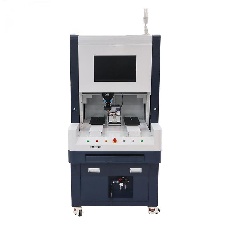
まず最初に, smartphone and tablet PCBs feature dense, tiny components (01005 packages, IC chips) vulnerable to mechanical stress. The Inline PCB Laser Depaneling Machine uses UV laser (355nm) for non-contact cutting, avoiding physical damage to components.
さらに, it achieves cutting accuracy ±0.02mm, matching the narrow routing gaps of 3C PCBs. 例えば, a smartphone factory used it to cut flexible PCBs (FPCs) for display modules, eliminating burrs and reducing component failure rates by 40%. さらに, it supports curved and irregular cutting paths, adapting to custom PCB designs.
Wearable Device PCB Processing: Handling Ultra-Small Form Factors
Wearable devices (smartwatches, earbuds) use ultra-small PCBs with tight space constraints. The Inline PCB Laser Depaneling Machine processes PCBs as small as 10mm×10mm with high thermal stability, avoiding PCB warpage.
さらに, its inline design syncs with SMT production lines, enabling continuous cutting without manual transfer. Besides, it generates minimal dust and noise, complying with 3C cleanroom requirements. This solution helped a wearable factory improve PCB yield by 35% and shorten production lead times by 25%.
Laptop & Peripheral PCB Depaneling: Boosting Throughput
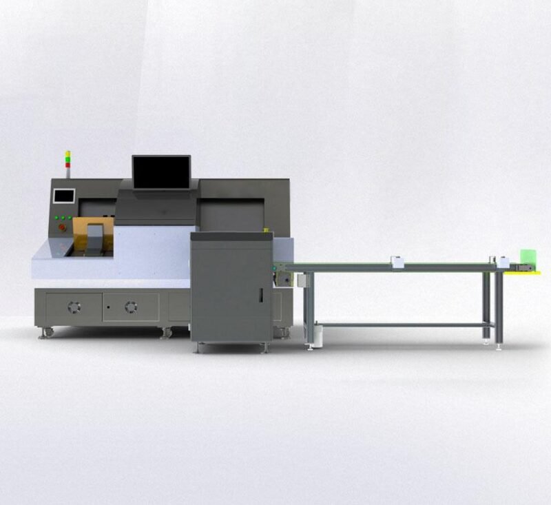
第二に, ラップトップ, keyboards, and USB devices demand high-volume PCB production. The Inline PCB Laser Depaneling Machine achieves cutting speeds up to 500mm/s, handling 1000+ PCBs per hour for mass production.
さらに, it supports multi-panel cutting, separating 8-12 PCBs from a single panel in one pass. For instance, a laptop factory used it to cut motherboard PCBs, reducing per-unit processing time by 30% and lowering labor costs. Consequently, it aligns with 3C electronics’ high-throughput production rhythms.
Flexible PCB (FPC) & Rigid-Flex PCB Cutting: Ensuring Flexibility
3C devices increasingly use FPCs and rigid-flex PCBs for space-saving. The Inline PCB Laser Depaneling Machine adjusts laser power dynamically to cut flexible and rigid layers without damaging the flexible substrate.
さらに, it avoids mechanical stress that causes FPC creasing or conductor breakage. さらに, it integrates with vision positioning systems to correct PCB offset in real time. A 3C accessory factory used it to process rigid-flex PCBs for wireless chargers, improving FPC bending durability by 50%.
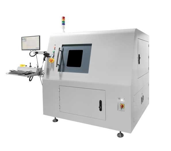
Smart Factory Integration: Streamlining Automated Workflows
ついに, modern 3C factories pursue fully automated production. The Inline PCB Laser Depaneling Machine connects to MES and AOI systems via Ethernet, enabling real-time data sharing and defect tracing.
Besides, it stores 200+ cutting profiles for different 3C PCB models, supporting quick model switching in seconds. さらに, it features self-diagnostic functions to reduce downtime. 例えば, a smart 3C factory used it to build a closed-loop PCB processing line, cutting overall production errors by 28%.
コアバリュー: Precision & Efficiency for 3C PCB Manufacturing
The Inline PCB Laser Depaneling Machine combines non-contact cutting, high precision, and inline compatibility. It adapts to diverse 3C PCB types—rigid, flexible, ultra-small—with tailored laser parameters.
Compared to mechanical depaneling tools, it eliminates component damage and burrs, ensuring consistent quality. Ultimately, it is not just a cutting tool but a solution that drives 3C electronics toward miniaturization and high-efficiency production.
Jetronl Instruments Co., Ltd. 電子計測分野に特化してきました。 35 年, 電子産業チェーン全体にわたるさまざまな測定ニーズをカバーし、正確な測定サポートを提供します.