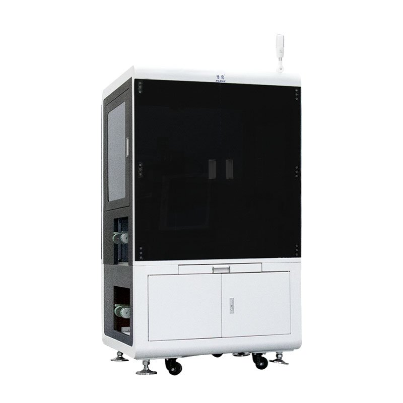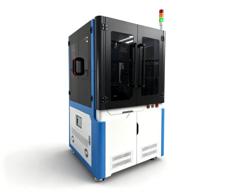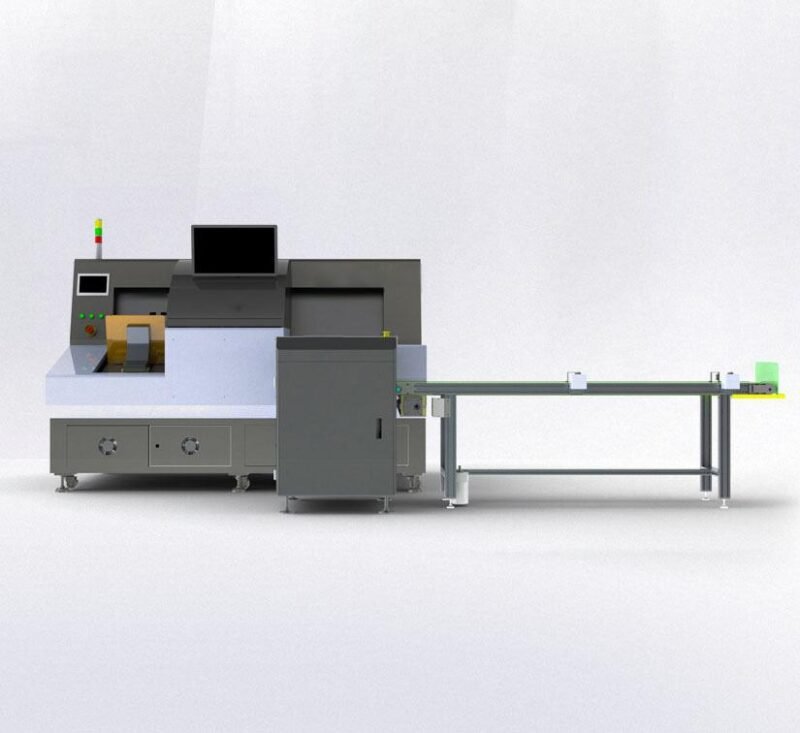
การผลิตเซมิคอนดักเตอร์และบรรจุภัณฑ์จำเป็นต้องมีการควบคุมข้อบกพร่องอย่างเข้มงวด, และ อุปกรณ์ตรวจสอบด้วยภาพสี่ด้านชิปอัตโนมัติ เป็นเครื่องมือหลัก. It checks all four sides of chips simultaneously, solving hidden defect issues that threaten product reliability.
Wafer Dicing Stage: Detecting Post-Dicing Defects
ประการแรก, wafer dicing often causes micro-cracks, chipping, or edge burrs on chip sides. The Automatic Chip Four-Side Visual Inspection Equipment uses high-resolution cameras to capture these flaws at the dicing stage.
นอกจากนี้, it integrates with dicing machines for real-time inspection, triggering alerts immediately when defects are found. This solution prevents defective chips from entering the next process, reducing wafer material waste by 30%.
Chip Packaging: Ensuring Lead & Bump Integrity
During packaging, chip leads (pins) or solder bumps may have deformation, missing parts, or oxidation. The Automatic Chip Four-Side Visual Inspection Equipment inspects these key structures from all four angles.
นอกจากนี้, it supports multi-chip package (MCP) inspection, adapting to complex packaging designs. Engineers use this data to adjust packaging parameters, solving issues like poor solderability that cause assembly failures.
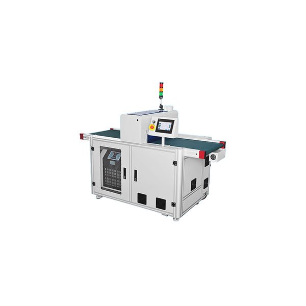
High-Speed Production Lines: Matching Mass Manufacturing Needs
ประการที่สอง, semiconductor factories run high-speed production lines that require fast inspection. The Automatic Chip Four-Side Visual Inspection Equipment achieves inspection speeds of up to 1200 chips per minute.
นอกจากนี้, its AI-powered image processing reduces false positives by 45% compared to traditional systems. This solution balances speed and accuracy, meeting the throughput requirements of mass chip production.
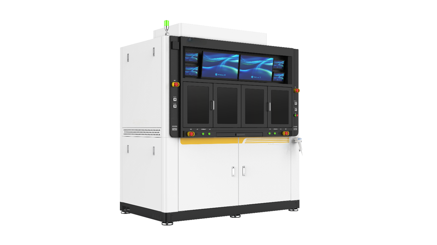
Advanced Semiconductor Chips: Adapting to Miniaturization
Miniaturized chips (เช่น, 3nm, 2nm process) have smaller features that are harder to inspect. The Automatic Chip Four-Side Visual Inspection Equipment uses ultra-high-definition (UHD) lenses and multi-spectrum lighting.
ตัวอย่างเช่น, it detects sub-micron-level scratches on 3nm chip sides that are invisible to standard equipment. This solution supports the development of advanced semiconductors, ensuring quality in cutting-edge processes.
การควบคุมคุณภาพ & Traceability: Meeting Industry Standards
ในที่สุด, semiconductor manufacturers need traceable quality data to comply with ISO and automotive-grade standards. The Automatic Chip Four-Side Visual Inspection Equipment logs inspection results for each chip.
Its data integration function connects to factory MES systems, creating a complete quality audit trail. This solution solves traceability challenges, helping manufacturers meet strict industry certification requirements.
ค่านิยมหลัก: Safeguarding Semiconductor Quality & ประสิทธิภาพ
The Automatic Chip Four-Side Visual Inspection Equipment combines 360° inspection capability, high speed, and AI intelligence. It replaces manual inspection, eliminating human error and reducing labor costs.
In semiconductor manufacturing and packaging, it’s not just inspection equipment—it’s a solution that ensures chip reliability, accelerates production, and supports the growth of the global semiconductor industry.
บริษัท เจทรอน อินสทรูเมนท์ส จำกัด, จำกัด. มีความเชี่ยวชาญในด้านการวัดทางอิเล็กทรอนิกส์สำหรับ 35 ปี, ครอบคลุมความต้องการการวัดที่หลากหลายทั่วทั้งห่วงโซ่อุตสาหกรรมอิเล็กทรอนิกส์ และให้การสนับสนุนการวัดที่แม่นยำ.