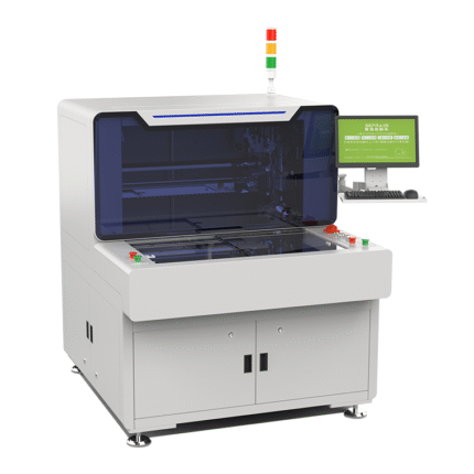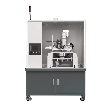
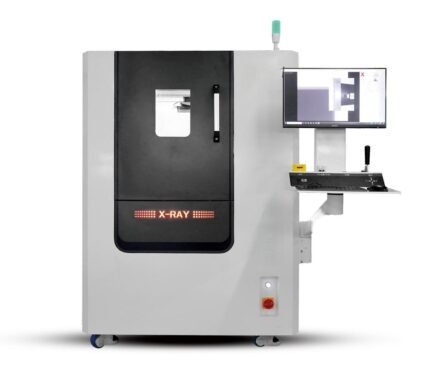
2.5D X線検査装置
2.5D X-RAY Inspection Equipment is an advanced non-destructive testing device that combines partial features of 2D and 3D X-RAY inspection. It can provide more comprehensive internal structure information than traditional 2D X-RAY equipment, while avoiding the higher cost and more complex operation of full 3D X-RAY systems.
コア機能
Enhanced 2D Imaging with Depth Sensing: It not only generates clear 2D projection images of the tested object (例えば, electronic components, プリント基板) but also uses technologies like layered scanning or tomosynthesis to capture depth-related information. This allows distinguishing defects or structures at different vertical layers (例えば, differentiating solder joints on upper and lower layers of a multi-layer PCB).
Precise Dimensional Measurement: Based on depth-sensing data, it can accurately measure key 3D-related dimensions that 2D systems cannot, such as the height of solder bumps, the thickness of internal material layers, and the vertical distance between components—with measurement accuracy up to ±1 μm.
Targeted Defect Detection: Focuses on detecting “quasi-3D” defects that are difficult to identify with 2D X-RAY, such as uneven solder joint height, partial delamination of semiconductor packages, and voids distributed in specific vertical layers of batteries.
主な技術的特徴
Balanced Performance & 料金: Offers depth-aware inspection capabilities closer to 3D systems, while having a lower purchase and maintenance cost than full 3D X-RAY equipment, making it suitable for medium-to-high precision testing needs.
Efficient Scanning: Adopts rapid layered scanning technology, with inspection speed 2–3 times faster than full 3D tomography, ensuring compatibility with batch production lines (例えば, PCB assembly, 半導体パッケージング).
Intuitive Data Analysis: Equipped with dedicated software that overlays depth information onto 2D images (例えば, color-coded depth maps) or generates cross-sectional views at arbitrary positions, enabling operators to quickly locate and evaluate internal defects.
幅広い互換性: Supports testing of various products, including small electronic components (BGA, CSP), multi-layer PCBs, lithium-ion battery cores, and precision mechanical parts—with adjustable X-ray parameters to adapt to different material thicknesses (0.1 mm–10 mm).
代表的な応用分野
Electronics Manufacturing: Inspecting solder joint quality (height, void rate) of multi-layer PCB components, detecting internal short circuits/layer misalignment of flexible PCBs.
半導体パッケージング: Evaluating the bonding quality of chip-on-board (COB) packages, checking delamination between semiconductor die and substrate, and measuring the height of solder balls in flip-chip packages.
Battery Production: Detecting voids in the electrode layers of lithium-ion batteries, verifying the alignment of internal tabs, and inspecting the uniformity of electrolyte distribution (in semi-transparent battery cases).

2.5D X線検査装置