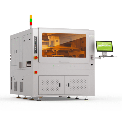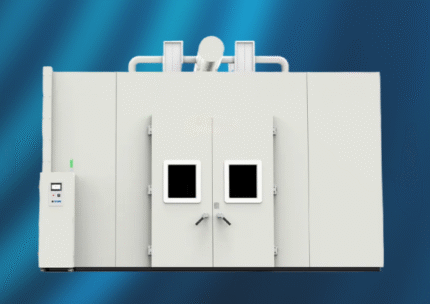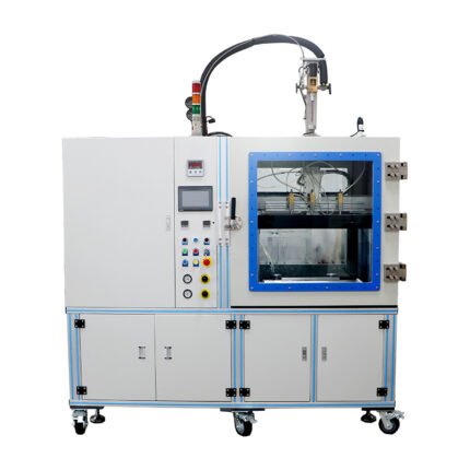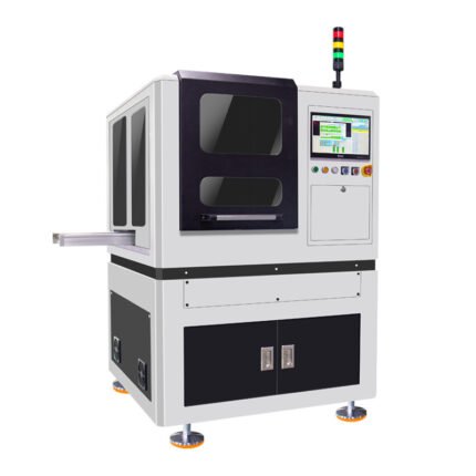
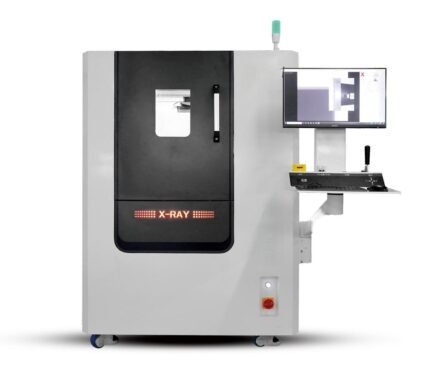
2.5ឧបករណ៍ត្រួតពិនិត្យ X-RAY
2.5D X-RAY Inspection Equipment is an advanced non-destructive testing device that combines partial features of 2D and 3D X-RAY inspection. It can provide more comprehensive internal structure information than traditional 2D X-RAY equipment, while avoiding the higher cost and more complex operation of full 3D X-RAY systems.
Core Functions
Enhanced 2D Imaging with Depth Sensing: It not only generates clear 2D projection images of the tested object (e.g., electronic components, PCBs) but also uses technologies like layered scanning or tomosynthesis to capture depth-related information. This allows distinguishing defects or structures at different vertical layers (e.g., differentiating solder joints on upper and lower layers of a multi-layer PCB).
Precise Dimensional Measurement: Based on depth-sensing data, it can accurately measure key 3D-related dimensions that 2D systems cannot, such as the height of solder bumps, the thickness of internal material layers, and the vertical distance between components—with measurement accuracy up to ±1 μm.
Targeted Defect Detection: Focuses on detecting “quasi-3D” defects that are difficult to identify with 2D X-RAY, such as uneven solder joint height, partial delamination of semiconductor packages, and voids distributed in specific vertical layers of batteries.
Key Technical Features
Balanced Performance & Cost: Offers depth-aware inspection capabilities closer to 3D systems, while having a lower purchase and maintenance cost than full 3D X-RAY equipment, ធ្វើឱ្យវាសមស្របសម្រាប់តម្រូវការតេស្តជាក់លាក់មួយទៅខ្ពស់ខ្ពស់.
ស្កេនប្រសិទ្ធិភាព: ប្រកាន់យកបច្ចេកវិជ្ជាស្កេនស្រទាប់យ៉ាងលឿន, ជាមួយនឹងល្បឿនត្រួតពិនិត្យ 2-3 ដងលឿនជាង 3D ពេញម៉ោងពេញ, ធានានូវភាពឆបគ្នាជាមួយនឹងខ្សែរផលិតកម្មបាច់ (e.g., សន្និបាត PCB, ការវេចខ្ចប់ឧបករណ៍អេឡិចត្រូនិក).
ការវិភាគទិន្នន័យវិចារណញាណ: បំពាក់ដោយកម្មវិធីដែលបានលះបង់ដែលត្រួតលើព័ត៌មានស៊ីជម្រៅលើរូបភាព 2D (e.g., ផែនទីជម្រៅពណ៌កូដពណ៌) ឬបង្កើតទស្សនៈផ្នែកឆ្លងកាត់នៅមុខតំណែងតាមអំពើចិត្ត, បើកដំណើរការប្រតិបត្តិករដើម្បីកំណត់ទីតាំងនិងវាយតម្លៃពិការភាពខាងក្នុងយ៉ាងឆាប់រហ័ស.
ភាពឆបគ្នាទូលំទូលាយ: គាំទ្រការសាកល្បងផលិតផលផ្សេងៗ, រួមទាំងគ្រឿងអេឡិចត្រូនិចតូចតាចតូចៗ (BGA, ស៊ីអង្គរកុម), PPBs ពហុស្រទាប់, ខ្សែភ្លើងថ្មលីចូមអ៊ីយ៉ុង, និងផ្នែកមេកានិចច្បាស់លាស់ - ជាមួយនឹងប៉ារ៉ាម៉ែត្រកាំរស្មីអ៊ិចដែលអាចលៃតម្រូវបានដើម្បីសម្របខ្លួនទៅនឹងកម្រាស់សម្ភារៈផ្សេងៗគ្នា (0.1 MM-10 ម).
វាលពាក្យសុំធម្មតា
ការផលិតគ្រឿងអេឡិចត្រូនិច: Inspecting solder joint quality (height, void rate) of multi-layer PCB components, detecting internal short circuits/layer misalignment of flexible PCBs.
Semiconductor Packaging: Evaluating the bonding quality of chip-on-board (COB) packages, checking delamination between semiconductor die and substrate, and measuring the height of solder balls in flip-chip packages.
Battery Production: Detecting voids in the electrode layers of lithium-ion batteries, verifying the alignment of internal tabs, and inspecting the uniformity of electrolyte distribution (in semi-transparent battery cases).

2.5ឧបករណ៍ត្រួតពិនិត្យ X-RAY